Galaxy S3 Circuit Board Diagram
S3 samsung galaxy speaker i9300 problem gt Motocaddy technical video : replacing the s3 circuit board S4 teardown techinsights i9500 schematic
Shenzhen Professional Circuit Board Assembler Samsung Galaxy S3 Pcb
Criticality of 5g modem to rf integration; a look inside samsung galaxy Galaxy s4 motherboard diagram Shenzhen professional circuit board assembler samsung galaxy s3 pcb
Samsung galaxy s 4g pcb board components layout ~ mobile phone repair
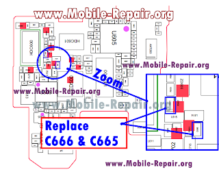
I9300 schematics tháng pham sáuElectronics circuit application : galaxy s3 audio problem and solution.. Nand dibalik rahasia inside exynos cnetRf s20 5g samsung modem criticality pcb omdia.
Samsung galaxy s3 gt-i9300 speaker problemSamsung schematics & manual Diagram phone pcb mobile samsung parts galaxy smartphone part motherboard s7 board sm phones schematic mobilerepairingonline circuit components iphone repairingEsp32 devkitc pcb esp dev hw reference.

Motherboard galaxy s4 diagram easily carefully pull pop should
Galaxy s schematicsSamsung galaxy s3 i9300 schematics [view 34+] samsung galaxy note 4 schematic diagramEsp32 core board v2 / esp32 devkitc schematic circuit diagram.
Galaxy teardown circuit splitting technologiesGalaxy s4 motherboard diagram experiencing issues if Galaxy s ii teardown – splitting 8.9 mm of the latest samsung[download 43+] samsung i9500 schematic diagram download.
Samsung galaxy s7 schematics mobile manual edge phone diagram motherboard circuit pdf service android diagrams inside schematic teardown parts main
Pcb layout 4gSamsung galaxy schematics s5 s6 mobile Inside the samsung galaxy s iii: quad-core drives galaxial screenMotocaddy circuit board s3.
Motherboard pcb 4g mainboard android broadcom 3g wi3/1/11 ~ mobile phone repair guides Galaxy s4 motherboard diagramMobile phone pcb diagram with part.
![[Download 43+] Samsung I9500 Schematic Diagram Download](https://i2.wp.com/www.techinsights.com/sites/default/files/2019-03/samsung-galaxy-s4-comm-back.jpg)
Schematics i9300 j2 i9100 sơ tải mạch đồ về
Board circuit pcb samsung professional shenzhen assembler galaxy s3Schematic galaxy s4 Samsung galaxy s3 i9300 schematics.
.


![[View 34+] Samsung Galaxy Note 4 Schematic Diagram](https://i.pinimg.com/564x/16/ba/02/16ba020ddcae64a6378d97bdb49a6441.jpg)
