Jk Ff Circuit Diagram
Draw the circuit diagram of jk ff using nand gates. derive its Ff jk vhdl slave flop synthesis courses flip master system circuit Jk flop flip circuit diagram master rgpv mca
[Solved] design sequential circuit using JK FF Design a sequential
Design of sequential circuits using jk &t ffs Jk flip two circuit following active low clear timing diagram flops uses aa solved Counter asynchronous flop jk triggered binary timing explain outputs
Jk circuit
Dff implement circuits(pdf) data analysis: results and discussion of different flip flop Jk tnxDigital electronics and logic design: master slave jk ff.
[solved] design sequential circuit using jk ff design a sequentialCircuit jk circuitlab description Flip jk flop circuit sequential input equation usingRgpv mca: master jk flip flop circuit diagram.

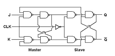
Courses:system_design:synthesis:master-slave_flip-flop:jk-ff [vhdl-online]
Freq divider jk ffDraw the circuit diagram of jk ff using nand gates. derive its Flip flop jk slave master circuit diagram ares fig fig14Jk ff condition race using diagram around avoiding nand.
Jk memory logic utilization flopSolved for the following circuit that uses two jk flip flops T-ff to jk-ffInput equation of sequential circuit using jk flip flop(हिन्दी ).

B): logic circuit diagram of memory element for jk-ff at 75%
Sequential usingJk table excitation flip flop equation characteristic ff state nand using draw derive circuit gates consider shown below need find Slave flop nand logic flops flipflop circuitverse constructedMultisim freq.
Draw and explain 3 bit asynchronous binary counter using positive edgeImplement a j-k ff using a dff .
![courses:system_design:synthesis:master-slave_flip-flop:jk-ff [VHDL-Online]](https://i2.wp.com/www.vhdl-online.de/_media/courses/system_design/synthesis/master-slave_flip-flop/folie340_jkffcircuit.svg?w=500&tok=5ddff5)


![[Solved] design sequential circuit using JK FF Design a sequential](https://i2.wp.com/www.coursehero.com/qa/attachment/13612392/)
